I started researching this, regarding phosphorus and carbon.
Gene expression
PLP has been implicated in increasing or decreasing the expression of certain genes. Increased intracellular levels of the vitamin lead to a decrease in the transcription of glucocorticoids. Also, vitamin B6 deficiency leads to the increased gene expression of albumin mRNA. Also, PLP influences expression of glycoprotein IIb by interacting with various transcription factors. The result is inhibition of platelet aggregation.
Following a little more with the search, PLP mentions the albumin.

Albumin - Wikipedia
Albumins in general are transport proteins that bind to various ligands and carry them around. Human types include:
- Human serum albumin is the main protein of human blood plasma. It makes up around 50% of human plasma proteins. It binds water, cations (such as Ca2+, Na+ and K+), fatty acids, hormones, bilirubin, thyroxine (T4) and pharmaceuticals (including barbiturates). Its main function is to regulate the oncotic pressure of blood. The isoelectric point of albumin is 4.9.
- Alpha-fetoprotein (alpha-fetoglobulin) is a fetal plasma protein that binds various cations, fatty acids and bilirubin.
- Vitamin D-binding protein binds to vitamin D and its metabolites, as well as to fatty acids.
- Not much is known about afamin. It seems to carry lipidated Wnt proteins and Vitamin E around.
- Extracellular matrix protein 1 is a less canonical albumin. It regulates bone mineralization.
It is interesting to note the isoelectric point.
Isoelectric point - Wikipedia
The isoelectric point (pI, pH(I), IEP), is the pH at which a molecule carries no net electrical charge or is electrically neutral in the statistical mean. The standard nomenclature to represent the isoelectric point is pH(I). However, pI is also used. For brevity, this article uses pI. The net charge on the molecule is affected by pH of its surrounding environment and can become more positively or negatively charged due to the gain or loss, respectively, of protons (H+).
Now:
Q: (L) Okay. I am stumped. I can't go any further now. On another subject, Ark read that phosphorus is in DNA structure. Could you comment?
A: How about if you comment on the relationship of phosphorous to you?
Q: (L) I don't know. Is there some relationship between phosphorous and carbon?
A: Well, that is not where we were leading.
Q: (L) Well, phosphorous is an essential element for the brain.
A: Okay.
A: Do you want to invite Ark to the discussion?
Q: (L) Of course. (A) What is the function of DNA, other than coding protein production?
A: Conductor of electricity.
Q: (L) Is that the only other function?
A: Well, as you know, electrical energy can have nearly endless applications. Examples... radio waves, neuro-transceiver for thought pattern programs facilitated through electromagnetic wave transmission, etc. Method used for creation and maintenance of program illusions, such as the perception of linear time as reality.
I have the impression that the alteration in our DNA resides in how certain enzymes and proteins can change the electrical potentials of our brain. Especially our cortex. If DNA is a conductor of electricity, I think it could be attributed to the same formula used for a copper wire that connects all the appliances in our house.
This is:
Calculation of the electrical resistance according to the type and shape of the conductor .
We know that an electric current is a flow of electrons. When moving through a conductor, the electrons must overcome a resistance; in metal conductors, this resistance comes from collisions between the electrons. If the passage is expedited and fluid, the electrons will travel in an orderly fashion, with little resistance. On the contrary, if the path is too narrow or too long, the electrons will crowd and collide with each other, producing, in addition, a lot of heat; they are opposed by a high resistance.
In a good conductor, who puts up low resistance, the electrons flow orderly, without colliding with each other.
In a bad electrical conductor, which offers high resistance to the flow of current, the electrons collide with each other because they cannot circulate freely and generate heat, which increases resistance. It is called electrical resistance to the opposition or difficulty that a current encounters when passing through a closed electrical circuit, and which allows the free flow of electrons to be slowed down or attenuated.
The unit of resistance is the ohm (W or Ω): and ohm is the resistance offered by a conductor when an ampere (current) flows through it and there is a difference of potential (voltage) of one volt between its ends.
Physically, any device or material inserted in an electric circuit represents in itself a resistance to the circulation of electric current, and depending on the characteristics of such device or material, the resistance to an electric current can be increased or decreased.
Therefore, the electrical resistance of a conductor depends on the nature of the material, its length and section, as well as the temperature.
The longer it is, the greater the resistance. The larger the section, the less resistance. The higher the temperature, the greater the resistance.
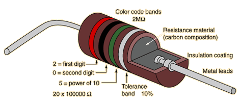
But something else is missing. And this is where carbon comes in. In electronics, carbon is commonly used in the manufacture of RESISTORS.

Our DNA, if we see the analogy with its carbon bases this element depending on its molecular arrangement, can act as a resistance or as a semiconductor.
For example, graphene:

Graphene - Wikipedia
Graphene is a substance composed of pure carbon, with atoms arranged in a regular hexagonal pattern, similar to graphite. It is an almost transparent material. A sheet of one atom thick is about 200 times stronger than today's stronger steel, its density being more or less the same as that of carbon fiber, and about five times lighter than aluminum.
(I think Ark will find this interesting)
Graphene is a zero-gap semiconductor, because its conduction and valence bands meet at the Dirac points. The Dirac points are six locations in momentum space, on the edge of the Brillouin zone, divided into two non-equivalent sets of three points. The two sets are labeled K and K'. The sets give graphene a valley degeneracy of gv = 2. By contrast, for traditional semiconductors the primary point of interest is generally Γ, where momentum is zero. Four electronic properties separate it from other condensed matter systems.
However, if the in-plane direction is no longer infinite, but confined, its electronic structure would change. They are referred to as graphene nanoribbons. If it is "zig-zag", the bandgap would still be zero. If it is "armchair", the bandgap would be non-zero (see figure).
Graphene's hexagonal lattice can be regarded as two interleaving triangular lattices. This perspective was successfully used to calculate the band structure for a single graphite layer using a tight-binding approximation.
Electronic spectrum:
Electrons propagating through graphene's honeycomb lattice effectively lose their mass, producing quasi-particles that are described by a 2D analogue of the Dirac equation rather than the Schrödinger equation for spin-1⁄2 particles.
Other graphene properties:
- High thermal conductivity.
- High electrical conductivity.
- High elasticity (deformable).
- High hardness (resistance to being scratched).
- High resistance. Graphite is approximately 200 times stronger than steel, similar to the resistance of diamond, but is much lighter.
- It is more flexible than carbon fiber but just as light.
- It is not affected by ionizing radiation.
- It has a low Joule effect (heating by conducting electrons).
- For the same task, graphite consumes less electricity than silicon.
- It is capable of generating electricity by exposure to sunlight.
- Graphene is a practically transparent material.
- It is very dense and does not allow helium to pass through in gaseous form, however it does allow water to pass through, which, enclosed in a graphite container, shows an evaporation rate similar to that shown in an open container.
In essence the carbon in the DNA acts as a semiconductor or resistance or both. And if it is both, what we have at the molecular level is a highly complex and sophisticated TRANSITOR. The same but on a larger level, for the neurons. Because they have more data/current input and output points in their receptors than a transistor used in electronics.
To summarize: The genetic alteration had the effect of suppressing the high function of our cortex. If the ability to receive the information is not truncated our cortex should be running (processing and receiving information, not amount of use. A computer CPU may be using all the cores but may be processing with difficulty, or at low frequency. The higher the frequency, the faster the ability to process information and therefore the more data you can receive.) at full capacity. This has already been discussed in the forum and various publications. But the detail was not clear. At least for me... The suppressed DNA factors and the carbon-related enzyme could mean that a transistor function is not there. In electronics a transistor has four functions and there are four types:
Functions:
1) Amplifier
2) Oscillator,
3) switch or
4) rectifier functions.
Types:
1) Point contact transistor
2) Bipolar bonding transistor
3) Field effect transistor
4) Phototransistor.
The last one is important, because:
Phototransistors are sensitive to electromagnetic radiation at frequencies close to that of visible light; because of this their current flow can be regulated by the incident light. A phototransistor is essentially the same as a normal transistor, only it can work in 2 different ways:
As a normal transistor with the base current (IB) (common mode);
As a phototransistor, when the light incident on this element acts as a base current. (IP) (lighting mode).
What you can do with the phosphorus?
Tunable Photoinduced Carrier Transport of a Black Phosphorus Transistor with Extended Stability Using a Light-Sensitized Encapsulated Layer:
In this article, we propose a novel approach to demonstrate tunable photoinduced carrier transport of a few-layered black phosphorus (BP) field-effect transistor (FET) with extended air stability using a “light-sensitized ultrathin encapsulated layer”. Titanium suboxide (TiOx) ultrathin film (approximately 3 nm), which is an amorphous phase of crystalline TiO2 and can be solution processed, simultaneously exhibits the unique dual functions of passivation and photoinduced doping on a BP FET. The photoinduced electron transfer at TiOx/BP interfaces provides tunable n-type doping on BP through light illumination. Accordingly, the intrinsic hole-dominated transport of BP can be gradually tuned to the electron-dominated transport at a TiOx/BP FET using light modulation, with enhanced electron mobility and extended air stability of the device. The novel device structure consisting of a light-sensitized encapsulated layer with controllable and reversible doping through light illumination on BP exhibits great potential for the future development of stable BP-based semiconductor logic devices or optoelectronic devices.
I hope this helps.


